VI Probe — 13.56 MHz Mixed-Signal Acquisition
Overview
A high-frequency current/voltage probe designed at Atomic Semi to capture deterministic
samples at 13.56 MHz. The board takes a sense input, conditions it
through an analog front-end, and feeds an STM32 F4 with the HRTIM peripheral
configured at register level for sub-nanosecond timing precision. Samples stream to a host
over a structured serial protocol for waveform reconstruction.
Hardware
- MCU: STM32 F4 — HRTIM configured from scratch by writing directly to control registers; ADC sequence chained to HRTIM events for jitter-free sampling.
- Analog front-end: low-noise op-amps with controlled gain staging, anti-aliasing filter sized against the sample rate.
- Layout: four-layer KiCad PCB; isolated analog and digital ground domains, controlled return paths, decoupling sized against the loop area.
- Comms: COBS-framed Protobuf over USB CDC for streaming reconstructed samples to the host.
What I designed
- Schematic verification against the F4 reference manual and the ADC datasheets — tracing every net, resolving ERC errors, sanity-checking power-rail decoupling.
- The analog front-end (gain stages, anti-aliasing) and component selection driven by the noise / bandwidth budget.
- The mixed-signal layout — keeping the analog domain quiet and the digital switching contained.
- Driver and HAL code: HRTIM init, ADC injected sequence, DMA into a ping-pong buffer, COBS-Protobuf framing.
- Bring-up: rails first under current limit, then the F4 boot, then HRTIM waveform on the scope, then the analog front-end with a known input.
Why HRTIM
The default STM32 timers max out at the system clock (typically ~168 MHz on the F4) for the
coarse counter — but the resolution is limited to one tick. HRTIM uses a phase-locked
delay-line to interpolate within a tick, giving sub-nanosecond resolution. For a 13.56 MHz
target, that's the difference between a clean reconstruction and a sample budget that doesn't
close. Configuring it properly meant reading the HRTIM chapter of RM0090 cover-to-cover and
writing the registers by hand — the HAL doesn't expose all of them.
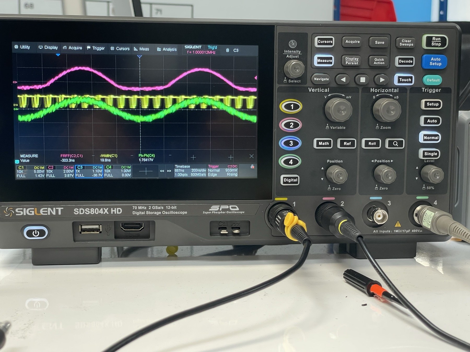
Status
Currently in bring-up — verifying the analog front-end's noise floor and the HRTIM-ADC synchronization on the bench. Schematic and PCB write-ups will go up here as they're cleared to publish.